ASML, in collaboration with Belgium’s imec, has opened a laboratory dedicated to testing the latest High NA Extreme Ultraviolet (EUV) lithography equipment.
Situated in Veldhoven, the Netherlands, the facility provides access to the first prototype High NA EUV scanner and associated processing and metrology tools.
Go deeper with GlobalData

ASML said the lab, which has been years in the making, is designed to assist logic and memory chip manufacturers, as well as advanced materials and equipment suppliers.
It offers these stakeholders an opportunity to de-risk the technology and develop proprietary High NA EUV use cases ahead of the scanners becoming operational in their production fabs.
ASML unveiled the £350m (€409.5m) chip making equipment earlier in 2024, to drive growth in artificial intelligence.
The lab’s resources, including a coat and development track, metrology tools, and wafer and mask handling systems, are also available to the broader ecosystem of material and equipment suppliers through imec’s High NA patterning programme.
How well do you really know your competitors?
Access the most comprehensive Company Profiles on the market, powered by GlobalData. Save hours of research. Gain competitive edge.

Thank you!
Your download email will arrive shortly
Not ready to buy yet? Download a free sample
We are confident about the unique quality of our Company Profiles. However, we want you to make the most beneficial decision for your business, so we offer a free sample that you can download by submitting the below form
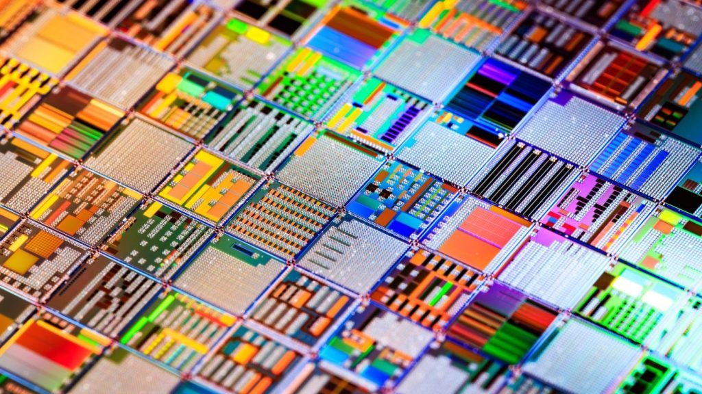
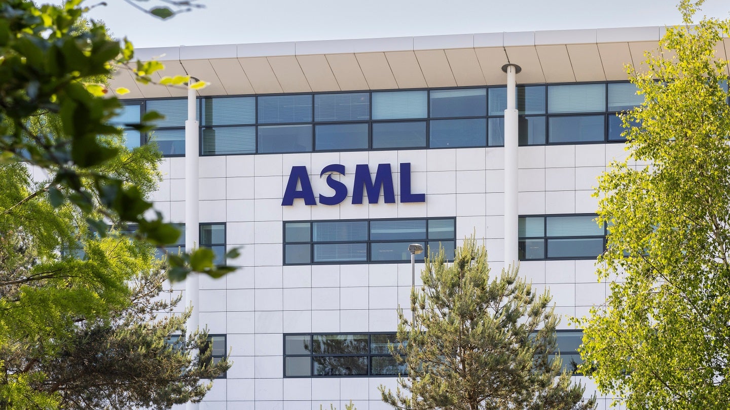
By GlobalDataASML, a dominant player in the lithography equipment market, provides technology that is crucial for creating the circuitry of chips.
Currently, only a handful of chip manufacturers such as TSMC, Samsung, Intel, and memory specialists SK Hynix and Micron, have the capability to manufacture using ASML’s existing EUV machines.
ASML president and CEO Christophe Fouquet said: “The ASML-imec High NA EUV Lithography Lab provides an opportunity for our EUV customers, partners and suppliers to access the High NA EUV system for process development while waiting for their own system to be available at their factories. This type of very early engagement with the ecosystem is unique and could significantly accelerate the learning curve on the technology and smoothen the introduction in manufacturing.”
The new chip-making equipment, promises up to 60% better resolution, potentially leading to the next generations of smaller, faster chips, according to Reuters.
ASML anticipates that its customers will start commercial manufacturing with the new tool between 2025 and 2026.
Imec president and CEO Luc Van den hove said: “High NA EUV is the next milestone in optical lithography, promising the patterning of metal lines/spaces with 20 nm pitch in one single exposure and enabling next generations of DRAM chips. This will improve yield and reduce cycle time and even CO₂ emissions compared to existing multi-patterning 0.33 NA EUV schemes. It will therefore be a key enabler to push Moore’s Law well into the ångström era. We are now thrilled to explore these capabilities in real life, using the prototype High NA EUV scanner.”