The technology industry continues to be a hotbed of patent innovation. Activity is driven by the increasing demand for high-resolution patterning, the need for precise manufacturing processes in nanoscale research and development, and the continuous advancements in electron beam lithography systems and software. The growing importance of technology such as electron beam column design, sophisticated beam control systems, advanced software algorithms for pattern generation, and precise stage positioning mechanisms is further driving innovation in the technology industry. In the last three years alone, there have been over 1.5 million patents filed and granted in the technology industry, according to GlobalData’s report on Innovation in technology: electron beam lithography. Buy the report here.

Access deeper industry intelligence
Experience unmatched clarity with a single platform that combines unique data, AI, and human expertise.
However, not all innovations are equal and nor do they follow a constant upward trend. Instead, their evolution takes the form of an S-shaped curve that reflects their typical lifecycle from early emergence to accelerating adoption, before finally stabilizing and reaching maturity.
Identifying where a particular innovation is on this journey, especially those that are in the emerging and accelerating stages, is essential for understanding their current level of adoption and the likely future trajectory and impact they will have.
185+ innovations will shape the technology industry
According to GlobalData’s Technology Foresights, which plots the S-curve for the technology industry using innovation intensity models built on over 1.6 million patents, there are 185+ innovation areas that will shape the future of the industry.
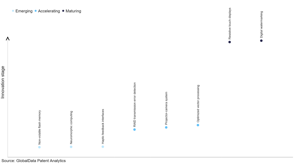
Within the emerging innovation stage, non-volatile flash memory, neuromorphic computing, and haptic feedback interfaces are disruptive technologies that are in the early stages of application and should be tracked closely. RAID transmission error detection, projector-camera system, and optimized vector processing are some of the accelerating innovation areas, where adoption has been steadily increasing. Among maturing innovation areas are resistive touch displays and digital watermarking, which are now well established in the industry.
Innovation S-curve for the technology industry

Electron beam lithography is a key innovation area in technology
Electron beam lithography is a precise method of nanofabrication that employs an electron beam to generate intricate patterns on various materials. It enables the production of high-resolution designs, down to a remarkable size of just 1 nanometer. This versatile technique finds application in fabricating detailed patterns across diverse materials such as metals, semiconductors, and polymers, contributing to advancements in fields like electronics, materials science, and nanotechnology.
GlobalData’s analysis also uncovers the companies at the forefront of each innovation area and assesses the potential reach and impact of their patenting activity across different applications and geographies. According to GlobalData, there are 65+ companies, spanning technology vendors, established technology companies, and up-and-coming start-ups engaged in the development and application of electron beam lithography.
Key players in electron beam lithography – a disruptive innovation in the technology industry
‘Application diversity’ measures the number of applications identified for each patent. It broadly splits companies into either ‘niche’ or ‘diversified’ innovators.
‘Geographic reach’ refers to the number of countries each patent is registered in. It reflects the breadth of geographic application intended, ranging from ‘global’ to ‘local’.
ASML is the leading patent filer in electron beam lithography. The company’s patents are aimed at invention describing a three-dimensional mask model that provides a more realistic approximation of the three-dimensional effects of a photolithography mask with sub-wavelength features than a thin-mask model. In one embodiment, the three-dimensional mask model includes a set of filtering kernels in the spatial domain that are configured to be convolved with thin-mask transmission functions to produce a near-field image.
In another embodiment, the three-dimensional mask model includes a set of correction factors in the frequency domain that are configured to be multiplied by the Fourier transform of thin-mask transmission functions to produce a near-field image.
Other prominent patent filers in the space include Samsung Group and Taiwan Semiconductor Manufacturing.
By geographic reach, Lam Research leads the pack, followed by Hitachi and Nikon. In terms of application diversity, ASML holds the top position, followed by Samsung Group and Taiwan Semiconductor Manufacturing.
Electron beam lithography plays a pivotal role within the realm of nanofabrication and nanotechnology. Its ability to precisely manipulate and pattern materials at the nanoscale enables the production of advanced devices and structures with extraordinary precision and resolution. Electron beam lithography technique enables researchers and engineers to fabricate high-density features, intricate patterns, and miniaturized circuits, pushing the boundaries of what is achievable in nanoscale fabrication.
To further understand the key themes and technologies disrupting the technology industry, access GlobalData’s latest thematic research report on Technology.
Data Insights
From

The gold standard of business intelligence.
Blending expert knowledge with cutting-edge technology, GlobalData’s unrivalled proprietary data will enable you to decode what’s happening in your market. You can make better informed decisions and gain a future-proof advantage over your competitors.


